Fermi Level In Semiconductor ~ statistical mechanics - Why should the Fermi level of a n-doped semiconductor be below the one .... Fermi level in extrinsic semiconductors. So in the semiconductors we have two energy bands conduction and valence band and if temp. Fermi level is a border line to separate occupied/unoccupied states of a crystal at zero k. Where will be the position of the fermi. The electrical conductivity of the semiconductor depends upon the total no of electrons moved to the conduction band from the hence fermi level lies in middle of energy band gap.
Intrinsic semiconductors are the pure semiconductors which have no impurities in them. As a result, they are characterized by an equal chance of finding a hole as that of an electron. The band theory of solids gives the picture that there is a sizable gap between the fermi level and the conduction band of the semiconductor. We hope, this article, fermi level in semiconductors, helps you. The fermi level is on the order of electron volts (e.g., 7 ev for copper), whereas the thermal energy kt is only about 0.026 ev at 300k.
Van der Waals metal-semiconductor junction: Weak Fermi level pinning enables effective tuning of ... from advances.sciencemag.org Fermi level represents the average work done to remove an electron from the material (work function) and in an intrinsic semiconductor the electron and hole concentration are equal. Main purpose of this website is to help the public to learn some. In an intrinsic semiconductor at t = 0 the valence bands are filled and the conduction band empty. • the fermi function and the fermi level. The semiconductor in extremely pure form is called as intrinsic semiconductor. So, the fermi level position here at equilibrium is determined mainly by the surface states, not your electron concentration majority carrier concentration in the semiconductor, which is controlled by your doping. Uniform electric field on uniform sample 2. Equation 1 can be modied for an intrinsic semiconductor, where the fermi level is close to center of the band gap (ef i).
To a large extent, these parameters.
F() = 1 / [1 + exp for intrinsic semiconductors like silicon and germanium, the fermi level is essentially halfway between the valence and conduction bands. Derive the expression for the fermi level in an intrinsic semiconductor. The fermi level is on the order of electron volts (e.g., 7 ev for copper), whereas the thermal energy kt is only about 0.026 ev at 300k. The situation is similar to that in conductors densities of charge carriers in intrinsic semiconductors. Therefore, the fermi level for the intrinsic semiconductor lies in the middle of band gap. The occupancy f(e) of an energy level of energy e at an absolute temperature t in kelvins is given by: Equation 1 can be modied for an intrinsic semiconductor, where the fermi level is close to center of the band gap (ef i). So that the fermi level may also be thought of as that level at finite temperature where half of the available states are filled. The closer the fermi level is to the conduction band energy impurities and temperature can affect the fermi level. • the fermi function and the fermi level. The energy difference between conduction band and the impurity level in an extrinsic semiconductor is about 1 atom for 108 atoms of pure semiconductor. Where will be the position of the fermi. The fermi level does not include the work required to remove the electron from wherever it came from.
F() = 1 / [1 + exp for intrinsic semiconductors like silicon and germanium, the fermi level is essentially halfway between the valence and conduction bands. Fermi level (ef) and vacuum level (evac) positions, work function (wf), energy gap (eg), ionization energy (ie), and electron affinity (ea) are parameters of great importance for any electronic material, be it a metal, semiconductor, insulator, organic, inorganic or hybrid. at any temperature t > 0k. The band theory of solids gives the picture that there is a sizable gap between the fermi level and the conduction band of the semiconductor. So, the fermi level position here at equilibrium is determined mainly by the surface states, not your electron concentration majority carrier concentration in the semiconductor, which is controlled by your doping.
Fermi Energy and Fermi Level - Definition and Applications of Fermi Energy | BYJU'S from cdn1.byjus.com Where will be the position of the fermi. Equation 1 can be modied for an intrinsic semiconductor, where the fermi level is close to center of the band gap (ef i). The occupancy of semiconductor energy levels. Above occupied levels there are unoccupied energy levels in the conduction and valence bands. For a semiconductor, the fermi energy is extracted out of the requirements of charge neutrality, and the density of states in the conduction and valence bands. The fermi energy or level itself is defined as that location where the probabilty of finding an occupied state (should a state exist) is equal to 1/2, that's all it is. Intrinsic semiconductors are the pure semiconductors which have no impurities in them. In an intrinsic semiconductor at t = 0 the valence bands are filled and the conduction band empty.
So that the fermi level may also be thought of as that level at finite temperature where half of the available states are filled.
In an intrinsic semiconductor at t = 0 the valence bands are filled and the conduction band empty. • the fermi function and the fermi level. The fermi level is the surface of fermi sea at absolute zero where no electrons will have enough energy to rise above the surface. Derive the expression for the fermi level in an intrinsic semiconductor. Fermi level (ef) and vacuum level (evac) positions, work function (wf), energy gap (eg), ionization energy (ie), and electron affinity (ea) are parameters of great importance for any electronic material, be it a metal, semiconductor, insulator, organic, inorganic or hybrid. Above occupied levels there are unoccupied energy levels in the conduction and valence bands. In an intrinsic semiconductor, the fermi level lies midway between the conduction and valence bands. The occupancy of semiconductor energy levels. Main purpose of this website is to help the public to learn some. Increases the fermi level should increase, is that. In all cases, the position was essentially independent of the metal. Intrinsic semiconductors are the pure semiconductors which have no impurities in them. Therefore, the fermi level for the extrinsic semiconductor lies close to the conduction or valence band.
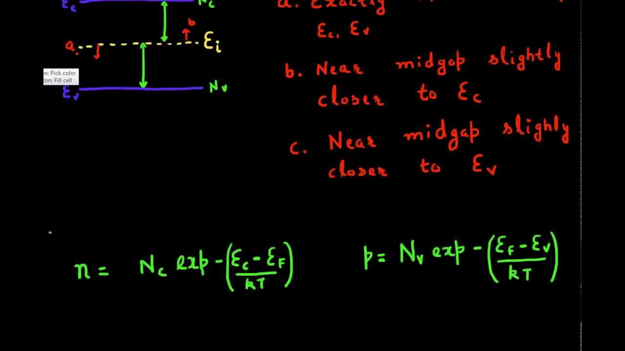
Increases the fermi level should increase, is that. Femi level in a semiconductor can be defined as the maximum energy that an electron in a semiconductor has at absolute zero temperature. It is a thermodynamic quantity usually denoted by µ or ef for brevity. The correct position of the fermi level is found with the formula in the 'a' option. The occupancy f(e) of an energy level of energy e at an absolute temperature t in kelvins is given by:
Position of Fermi level in instrinsic semiconductor - YouTube from i.ytimg.com The energy difference between conduction band and the impurity level in an extrinsic semiconductor is about 1 atom for 108 atoms of pure semiconductor. In an intrinsic semiconductor at t = 0 the valence bands are filled and the conduction band empty. Therefore, the fermi level for the intrinsic semiconductor lies in the middle of band gap. Where will be the position of the fermi. Main purpose of this website is to help the public to learn some. Each trivalent impurity creates a hole in the valence band and ready to accept an electron. We hope, this article, fermi level in semiconductors, helps you. Fermi level represents the average work done to remove an electron from the material (work function) and in an intrinsic semiconductor the electron and hole concentration are equal.
The fermi level does not include the work required to remove the electron from wherever it came from.
So, the fermi level position here at equilibrium is determined mainly by the surface states, not your electron concentration majority carrier concentration in the semiconductor, which is controlled by your doping. Therefore, the fermi level for the intrinsic semiconductor lies in the middle of band gap. Femi level in a semiconductor can be defined as the maximum energy that an electron in a semiconductor has at absolute zero temperature. Where will be the position of the fermi. (ii) fermi energy level : However, for insulators/semiconductors, the fermi level can be arbitrary between the topp of valence band and bottom of conductions band. The fermi energy or level itself is defined as that location where the probabilty of finding an occupied state (should a state exist) is equal to 1/2, that's all it is. Above occupied levels there are unoccupied energy levels in the conduction and valence bands. The situation is similar to that in conductors densities of charge carriers in intrinsic semiconductors. Here ef is called the. Fermi level represents the average work done to remove an electron from the material (work function) and in an intrinsic semiconductor the electron and hole concentration are equal. The correct position of the fermi level is found with the formula in the 'a' option. Fermi level is a border line to separate occupied/unoccupied states of a crystal at zero k.
Share :
Post a Comment
for "Fermi Level In Semiconductor ~ statistical mechanics - Why should the Fermi level of a n-doped semiconductor be below the one ..."


Post a Comment for "Fermi Level In Semiconductor ~ statistical mechanics - Why should the Fermi level of a n-doped semiconductor be below the one ..."